Printed Circuit Boards (PCBs) are essential components that bring electronic devices to life. They provide the platform for connecting and supporting various electronic parts. If you’re starting your journey in electronics, understanding the PCB design process will give you a strong foundation. Let’s explore the key stages involved. If you want to excel in this career path, then it is recommended that you upgrade your skills and knowledge regularly with the latest PCB Design Course in Bangalore.
What is PCB Design?
PCB design is the process of planning and arranging electronic components on a board so they can work together efficiently. It ensures proper electrical connections while also meeting mechanical and manufacturing requirements.
Step-by-Step PCB Design Process
1. Developing the Schematic
The design process begins with a schematic diagram, which represents the logical structure of the circuit.
Key activities:
- Selecting the required components
- Organizing them based on functionality
- Connecting them using symbolic representations
2. Component Selection
Choosing the right components is vital for the circuit’s performance and durability.
Factors to consider:
- Voltage and current specifications
- Physical size and packaging
- Cost and availability
- Operating reliability
3. Creating the PCB Layout
This stage converts the schematic into a physical board design.
What it involves:
- Placing components strategically
- Optimizing the use of available space
- Ensuring compatibility with the product design
It’s simpler to master this tool and progress your profession with the help of PCB Design Training which provide thorough instruction and job placement support to anyone seeking to improve their talents.
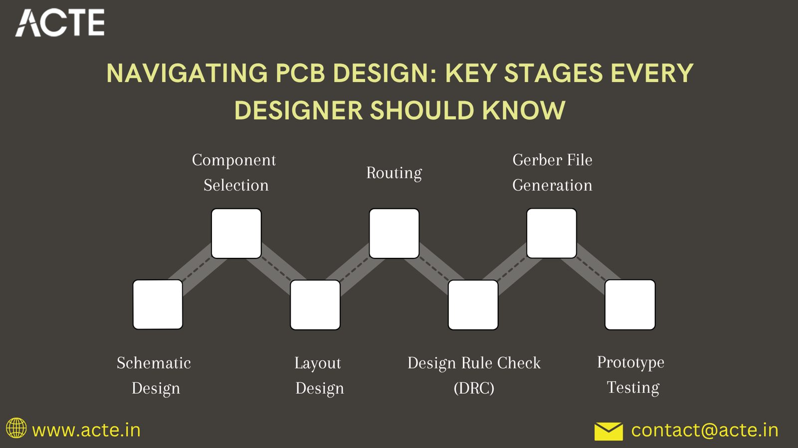
4. Routing the Connections
Routing involves creating conductive paths to connect components.
Important points:
- Maintaining appropriate trace width
- Reducing trace length for efficiency
- Minimizing noise and interference
5. Performing Design Rule Checks (DRC)
Before moving to production, the design is verified for errors.
This ensures:
- Proper spacing and dimensions
- Correct electrical connections
- Adherence to manufacturing standards
6. Generating Manufacturing Files
After validation, files required for production are created.
These include:
- PCB layer details
- Drill hole information
- Component placement data
7. Prototype and Testing
A prototype is built to test the real-world performance of the PCB.
The goal is to:
- Identify and fix issues
- Confirm proper functionality
- Improve the design before large-scale production
Conclusion
PCB design is a systematic process that requires accuracy and careful planning. By following each step, designers can create efficient and reliable circuit boards.
As technology continues to evolve, learning PCB design is a valuable skill that opens doors to many opportunities in the electronics industry.